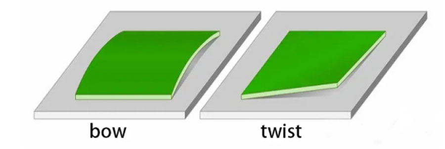
There are two main types of PCB warpage issues: bow and twist.

What is Bow?
Bow refers to the bending of the edges of a PCB, resulting in an arc-like convex or concave shape. This typically occurs along two opposite edges of the PCB, making the entire board resemble a bow, hence the name. Bowing can be either single-sided or double-sided.
Measurement Method
Place the PCB flat on a marble surface with all four corners touching the surface, then measure the height of the arch in the middle.
Calculation Method
Bow rate=Height of the Arch/Length of the PCB's long edge×100%
What is Twist?
Twist refers to the rotation occurring along the diagonal of a PCB, creating an elevation or depression along the diagonal. This results in the PCB having a twisted shape, hence the name.
Measurement Method
Place three corners of the PCB on a surface and measure the height of the corner that is elevated.
Calculation Method
Twist rate=Height of the raised single corner/Length of the diagonal of PCB * 100%.
Causes of PCB Warpage
1、Stress Exceeding Material Limits
When the stress applied to the PCB exceeds the material's tolerance, it leads to warpage. This stress often results from uneven forces such as non-uniform soldering temperatures or chemical impacts.
2、Thermal Stress
During manufacturing, uneven thermal stress, such as overheating during the reflow process, can cause PCB warpage. When the PCB reaches temperatures above its Tg (glass transition temperature), the material softens, leading to permanent deformation.
3、Chemical Stress
Chemical stress occurs when PCB materials are subjected to chemical erosion. Factors such as chemical solvents, humidity, and climate changes can impact the PCB material, resulting in warpage.
4、Improper Manufacturing Processes
Incorrect PCB design and manufacturing processes, such as uneven copper surface area distribution and overheating during production, can also lead to PCB warpage.
Reducing PCB Warpage During Design
1、Select Appropriate Materials
Choose materials with a high Tg (glass transition temperature). These materials exhibit better dimensional stability at high temperatures, reducing deformation due to thermal stress.
2、Increase Board Thickness
Without affecting overall product performance, increasing the PCB thickness can enhance its resistance to bending and warping.
3、Optimize PCB Design
Minimize the number and overall size of the PCB to reduce deformation from its own weight. Properly arrange component placement to avoid concentrating heavy components on one side, thereby reducing warpage issues.
4、Choose Suitable Layer Stack-Up
Opt for a symmetrical lamination process and appropriate stack-up to minimize internal stress imbalances.
5、Add Support Structures
Incorporate support structures such as additional connectors and support pillars in the PCB design to enhance structural strength and reduce the possiable of warpage.
Preventing PCB Warpage During Manufacturing
1、Reduce the Number of PCBs on Narrow Edges in Production Panels
Minimize the number of PCBs on the narrow edges of production panels to reduce warpage issues in the reflow oven. The reflow oven uses chains to move the boards, and larger panels are more prone to warpage. Place the long edge of the production panel on the reflow oven chain edges to reduce deformation on the narrow edge.
2、Use an Automatic Depaneling Machine
Manual separation of V-cut PCBs can damage the stress structure, leading to warpage. An automatic depaneling machine prevents this issue.
Advantages of Automatic Depaneling Machines
·No warpage occurs during the depaneling process.
·Eliminates the impact of manual depaneling on component soldering, reducing the risk of PCBA rejection.
·The depaneled PCBs have a smoother, burr-free appearance.
·Production panels are more stable during assembly due to better edge rail connections compared to half holes.
3、Bake PCBs Before Assembly
Baking PCBs before electronic assembly removes moisture and allows the resin in the laminate to cure fully, further eliminating residual stress and preventing warpage.
4、Control Manufacturing Temperatures:
Carefully control temperatures during the manufacturing process to avoid overheating the PCB, which can soften the material and cause permanent deformation.

Contact: Wing
Phone: +852 21386086
E-mail: sales@fwpcb.com
Whatsapp:+86 199 2764 2527
Add: Unit 3, 6/F., Kam Hon Industrial Building,8 Wang Kwun Road, Kowloon Bay, Hong Kong
We chat
